- 您现在的位置:买卖IC网 > Sheet目录3753 > ATMEGA169P-16MCHR (Atmel)MCU AVR 16KB FLASH 16MHZ 64-VQFN
PIC16F946
DS41265A-page 192
Preliminary
2005 Microchip Technology Inc.
16.1
Configuration Bits
The configuration bits can be programmed (read as
‘0’), or left unprogrammed (read as ‘1’) to select various
device configurations as shown in Register 16-1.
These bits are mapped in program memory location
2007h.
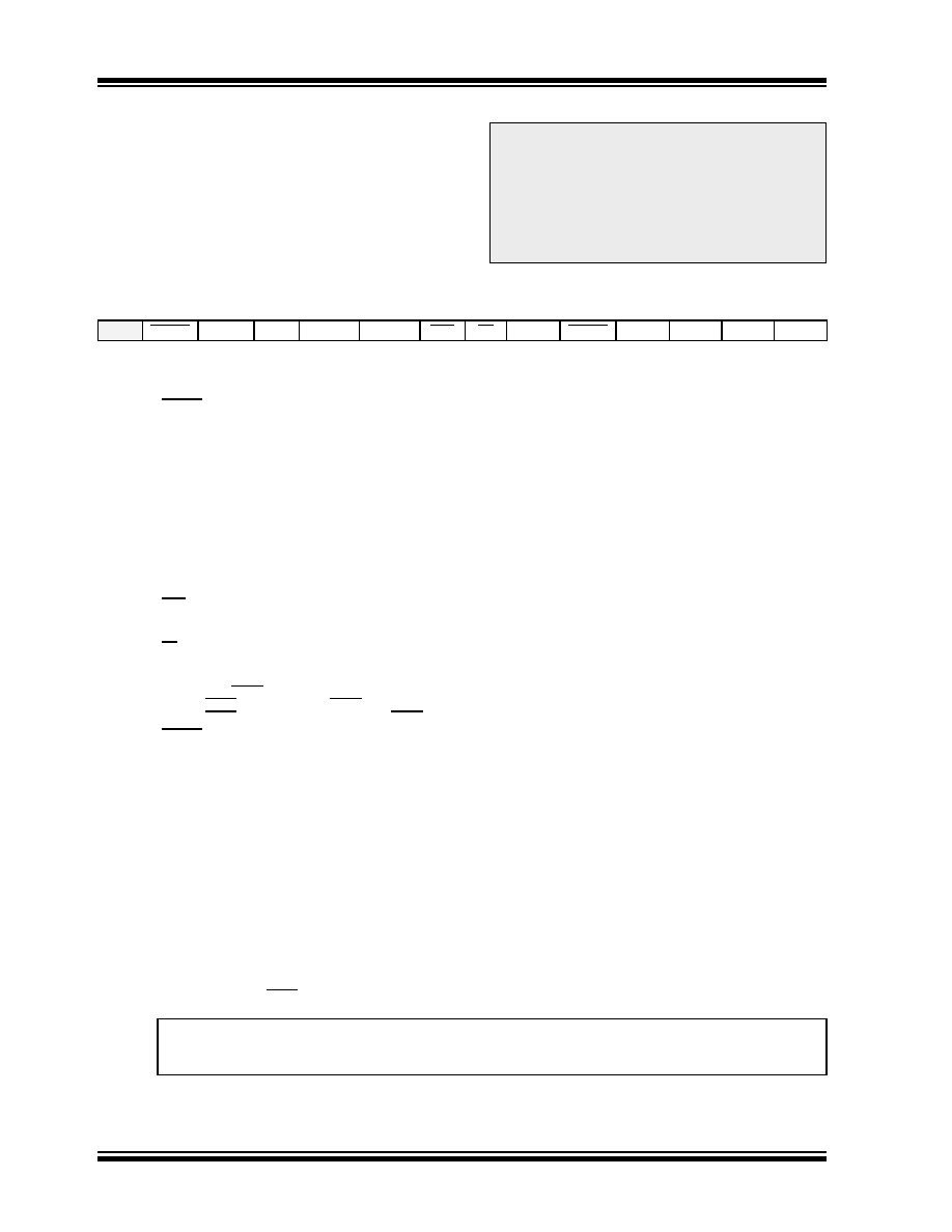
REGISTER 16-1:
CONFIG – CONFIGURATION WORD (ADDRESS: 2007h)
Note:
Address
2007h is
beyond the user
program memory space. It belongs to the
special
configuration
memory
space
(2000h-3FFFh), which can be accessed
only
during
programming.
See
“PIC16F91X/946 Memory Programming
Specification”
(DS41244)
for
more
information.
—DEBUG
FCMEN
IESO
BOREN1
BOREN0
CPD
CP
MCLRE
PWRTE
WDTE
FOSC2
FOSC1
FOSC0
bit 13
bit 0
bit 13
Unimplemented: Read as ‘1’
bit 12
DEBUG: In-Circuit Debugger Mode bit
1
= In-Circuit Debugger disabled, RB6/ICSPCLK/ICDCK/SEG14 and RB7/ICSPDAT/ICDDAT/SEG13 are general purpose I/O pins
0
= In-Circuit Debugger enabled, RB6/ICSPCLK/ICDCK/SEG14 and RB7/ICSPDAT/ICDDAT/SEG13 are dedicated to the debugger
bit 11
FCMEN: Fail-Safe Clock Monitor Enabled bit
1
= Fail-Safe Clock Monitor is enabled
0
= Fail-Safe Clock Monitor is disabled
bit 10
IESO: Internal External Switchover bit
1
= Internal External Switchover mode is enabled
0
= Internal External Switchover mode is disabled
bit 9-8
BOREN<1:0>: Brown-out Reset Selection bits(1)
11
= BOR enabled
10
= BOR enabled during operation and disabled in Sleep
01
= BOR controlled by SBOREN bit (PCON<4>)
00
= BOR disabled
bit 7
CPD: Data Code Protection bit(2)
1
= Data memory code protection is disabled
0
= Data memory code protection is enabled
bit 6
CP: Code Protection bit(3)
1
= Program memory code protection is disabled
0
= Program memory code protection is enabled
bit 5
MCLRE: RB3/MCLR/VPP pin function select bit(4)
1
= RB3/MCLR/VPP pin function is MCLR
0
= RB3/MCLR/VPP pin function is digital input, MCLR internally tied to VDD
bit 4
PWRTE: Power-up Timer Enable bit
1
= PWRT disabled
0
= PWRT enabled
bit 3
WDTE: Watchdog Timer Enable bit
1
= WDT enabled
0
= WDT disabled and can be enabled by SWDTEN bit (WDTCON<0>)
bit 2-0
FOSC<2:0>: Oscillator Selection bits
111
= RC oscillator: CLKO function on RA6/OSC2/CLKO/T1OSO pin, RC on RA7/OSC1/CLKI/T1OSI
110
= RCIO oscillator: I/O function on RA6/OSC2/CLKO/T1OSO pin, RC on RA7/OSC1/CLKI/T1OSI
101
= INTOSC oscillator: CLKO function on RA6/OSC2/CLKO/T1OSO pin, I/O function on RA7/OSC1/CLKI/T1OSI
100
= INTOSCIO oscillator: I/O function on RA6/OSC2/CLKO/T1OSO pin, I/O function on RA7/OSC1/CLKI/T1OSI
011
= EC: I/O function on RA6/OSC2/CLKO/T1OSO pin, CLKI on RA7/OSC1/CLKI/T1OSI
010
= HS oscillator: High-speed crystal/resonator on RA6/OSC2/CLKO/T1OSO and RA7/OSC1/CLKI/T1OSI
001
= XT oscillator: Crystal/resonator on RA6/OSC2/CLKO/T1OSO and RA7/OSC1/CLKI/T1OSI
000
= LP oscillator: Low-power crystal on RA6/OSC2/CLKO/T1OSO and RA7/OSC1/CLKI/T1OSI
Note
1:
Enabling Brown-out Reset does not automatically enable Power-up Timer.
2:
The entire data EEPROM will be erased when the code protection is turned off.
3:
The entire program memory will be erased when the code protection is turned off.
4:
When MCLR is asserted in INTOSC or RC mode, the internal clock oscillator is disabled.
Legend:
R = Readable bit
W = Writable bit
U = Unimplemented bit, read as ‘0’
- n = Value at POR
‘1’ = Bit is set
‘0’ = Bit is cleared
x = Bit is unknown
发布紧急采购,3分钟左右您将得到回复。
相关PDF资料
2-1546217-0
TERM BLK RCPT 20POS SIDE 5.08MM
1-1546217-9
TERM BLK RCPT 19POS SIDE 5.08MM
1-1546217-8
TERM BLK RCPT 18POS SIDE 5.08MM
1-1546217-7
TERM BLK RCPT 17POS SIDE 5.08MM
1-1546217-6
TERM BLK RCPT 16POS SIDE 5.08MM
1-1546217-5
TERM BLK RCPT 15POS SIDE 5.08MM
1-1546217-4
TERM BLK RCPT 14POS SIDE 5.08MM
1-1546217-3
TERM BLK RCPT 13POS SIDE 5.08MM
相关代理商/技术参数
ATMEGA169P-16MCU
功能描述:8位微控制器 -MCU AVR 16KB, 512B EE 16MHz 1KB SRAM, 5V
RoHS:否 制造商:Silicon Labs 核心:8051 处理器系列:C8051F39x 数据总线宽度:8 bit 最大时钟频率:50 MHz 程序存储器大小:16 KB 数据 RAM 大小:1 KB 片上 ADC:Yes 工作电源电压:1.8 V to 3.6 V 工作温度范围:- 40 C to + 105 C 封装 / 箱体:QFN-20 安装风格:SMD/SMT
ATMEGA169P-16MU
功能描述:8位微控制器 -MCU AVR 16K FLASH 512B EE 1K SRAM LCD ADC RoHS:否 制造商:Silicon Labs 核心:8051 处理器系列:C8051F39x 数据总线宽度:8 bit 最大时钟频率:50 MHz 程序存储器大小:16 KB 数据 RAM 大小:1 KB 片上 ADC:Yes 工作电源电压:1.8 V to 3.6 V 工作温度范围:- 40 C to + 105 C 封装 / 箱体:QFN-20 安装风格:SMD/SMT
ATMEGA169P-16MU SL383
制造商:Atmel Corporation 功能描述:MCU 8BIT ATMEGA RISC 16KB FLASH 3.3V/5V 64PIN MLF - Tape and Reel
ATMEGA169P-16MUR
功能描述:8位微控制器 -MCU AVR LCD 16KB FLSH EE 512B 1KB SRAM-16MHZ RoHS:否 制造商:Silicon Labs 核心:8051 处理器系列:C8051F39x 数据总线宽度:8 bit 最大时钟频率:50 MHz 程序存储器大小:16 KB 数据 RAM 大小:1 KB 片上 ADC:Yes 工作电源电压:1.8 V to 3.6 V 工作温度范围:- 40 C to + 105 C 封装 / 箱体:QFN-20 安装风格:SMD/SMT
ATMEGA169P-8AU
制造商:ATMEL 制造商全称:ATMEL Corporation 功能描述:Microcontroller with 16K Bytes In-System Programmable Flash
ATMEGA169P-8MU
制造商:ATMEL 制造商全称:ATMEL Corporation 功能描述:Microcontroller with 16K Bytes In-System Programmable Flash
ATMEGA169PA
制造商:ATMEL 制造商全称:ATMEL Corporation 功能描述:8-bit Microcontroller with 16K Bytes In-System Programmable Flash
ATMEGA169PA_1
制造商:ATMEL 制造商全称:ATMEL Corporation 功能描述:High Endurance Non-volatile Memory segments